UV LED PC Board Exposure Build
Building a UV Exposure Box with UV LEDs
There are many solutions available to expose the photo-resist of a PCB. Few, if any, can fully expose your board in 30 seconds or less. This UV Light Source is capable of exposing photo-resistor for the UV curing of different paints and finishes.
Photo exposing a PCB is a quick way to produce low-quantity designs and can be done by the experimenter at home relatively inexpensively. We recently had a client who wished to do exactly this but wanted the ability to rapidly expose and process numerous one-off designs but they required a UV light source to expose pre-sensitized boards.
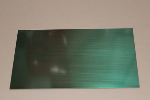
The board is made by MG Chemicals and is their Model 687. It is a Single Sided Pre-sensitized 1/32″ Copper Clad Board 100mm x 150mm (approximately 4″ x 6″). It comes pre-sensitized and incorporates a peel-off layer protecting the sensitized copper base.
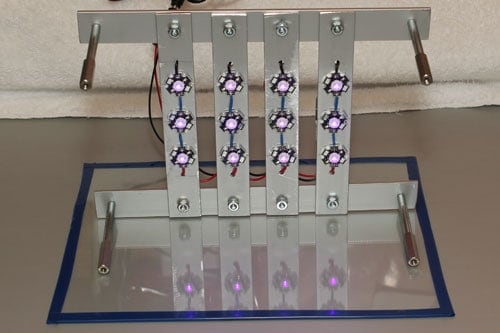
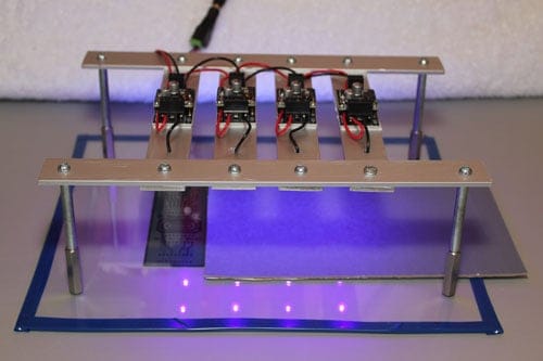
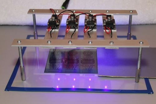
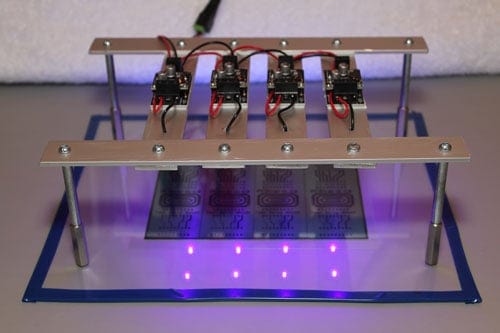
The solution they finally built and utilized was an exposer setup incorporating twelve 1 watt STAR UV LEDs. The twelve LEDs are divided into four parallel strings of three modules, each connected in series being driven by a 1W LED driver.
MG Chemicals sells a fluorescent light source for developing the boards, but it was deemed that this process was too slow and at the time, the client was not able to source this product. A little research shows the output frequency of the lamp is at 375nm and that generally, any emitted energy in the 350nm to 450nm range would be more than ample to expose the boards. The UV STAR LED selected for this project has an output frequency of 400nm to 410nm which was right in the center for the desired frequency spectrum.
After the exposure apparatus was assembled and the first test board was made, it was determined that an exposure time of between 15 to 20 seconds is all that was required to properly expose the board. There have been several other projects out there where 5mm UV LEDs were used, but those resulted in exposure times which varied from several minutes to tens of minutes depending on the quality of the LEDs use. At 15 to 20 seconds, this solution has given them that rapid prototype ability. Read on for the build process and see the unit in operation.
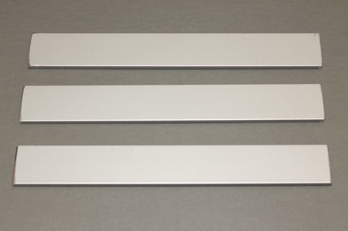
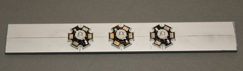
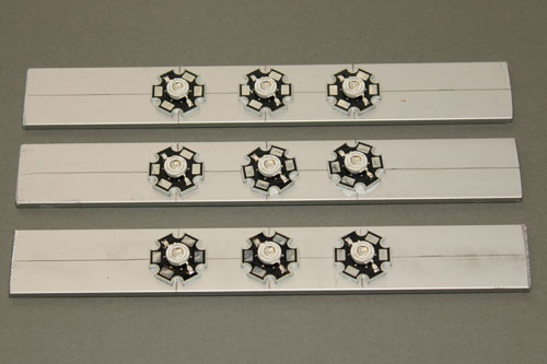
Each stringer holding the three STAR LEDs is constructed of 1″ wide by 1/8″ thick aluminum bar was trimmed to 7″ in length.
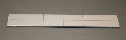
Marking each piece of aluminum for where the STAR LEDs will be positioned. Spacing between the three LEDs is 1 1/4″.
To mount the STAR LEDs to the aluminum, several options were reviewed. The most common way is to use two mounting holes per LED and includes a screw through the mount.
To dissipate the heat, a thermal compound between the LED and aluminum. If mounting this way, you need to ensure your mounting screws do not short out anything on the LED module.
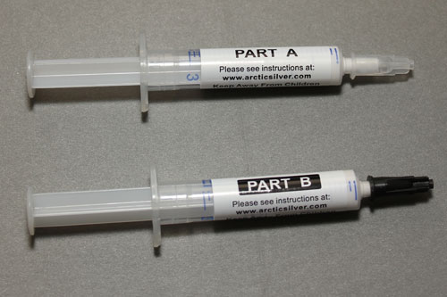
Another option that presented itself during the construction was to use a thermal adhesive. It would provide not only a secure adhesive to mount the STAR LED to the aluminum, but also a heat-transfer medium to transfer the heat away from the STAR LED.
A commonly available thermal adhesive is Arctic Silver Thermal Adhesive. It is a two-part permanent adhesive for thermal joints in minimum bond line applications. It is created with 99.8% pure micronized silver. 62% to 65% silver content by weight, has a wide temperature range (- 40C to >150C), and is formulated to conduct heat and not electricity.
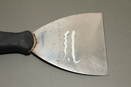
You will not need much compound to hold the STAR LED to the aluminum. Apply equal amounts from the Part A and Part B tubes onto a surface that can be used as a mixing platform. Use a surface that can be wiped clean or disposed of afterward.
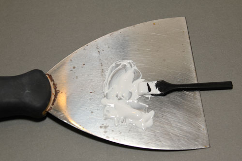
Now go ahead and mix Part A and Part B together. You want to get a good mix to ensure optimum adhesion.
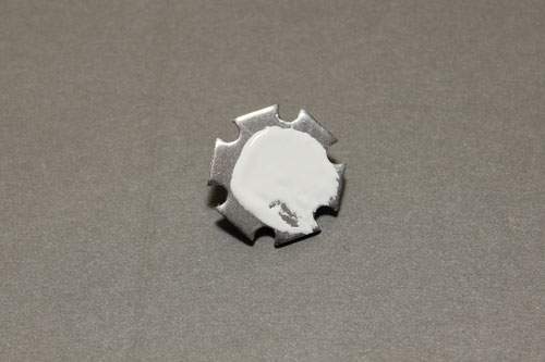
From the mix of Parts A and B, apply enough to cover the bottom of the STAR LED.
Position the STAR LEDs with the adhesive to the aluminum strip.
Now would be a good time to align the positive and negative terminals of the LEDs. The negative terminal of one LED should be positioned closest to the positive terminal of the next LED. This will allow you to run a simple, clean wire between each LED when it comes time to connect them together in series.
Each LED should be positioned tightly to the aluminum. Push it into place, and rotate slightly to spread the adhesive under each LED.
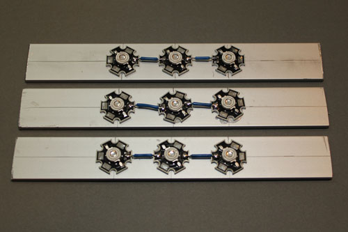
After allowing the adhesive to set (in this case, we let it sit overnight), you can go ahead and wire up the LEDs. By aligning the LEDs, you can easily connect them up in series.
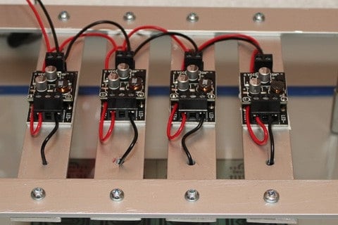
To drive the STAR LEDs, we used a 1watt driver. The driver is used to limit the current going to the LEDs, in this case, approximately 285mA.
Each support leg has three STAR LEDs on it, connected in series and run to the output of the 1watt driver. The driver is run from a 12v DC power adapter, with four of the drivers running from a single 12v 1A power supply.
The assembled frame has four cross pieces each which hold the three STAR LEDs and are 7″ in length which attached to a pair of support which is 10″ long. The support bars are spaced 1 1/2″ apart, with the LEDs being 1 1/4″ between each other. The legs selected were liberated from our junk-box and were made up of spacers that measured 3 1/4″ long.
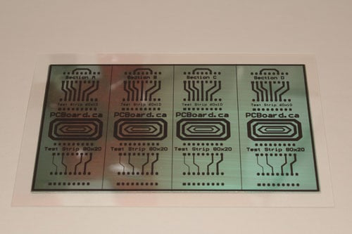
You now need to prepare your image to be transferred to a PCB. The image you create will be of the traces for your PCB design. It should be printed on clear acetate or more commonly overhead/transparency material.
This can be printed on either an inkjet or a laser printer. Your artwork should by 1:1 and is a Positive image (where you want traces, you should have ink covering that area). Try and print your design out at a high resolution to eliminate jagged lines.
For this sample, it was printed out at 300dpi on an inkjet printer. The blacks are very black coverage density is great.
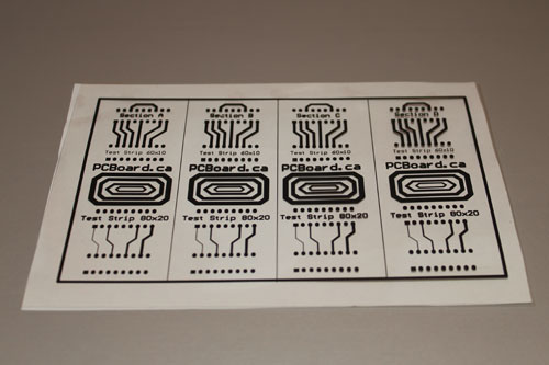
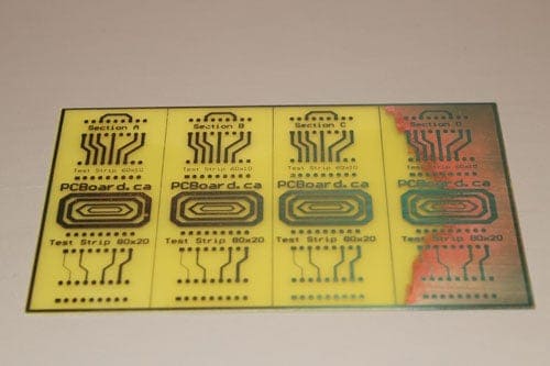
The design shown was created as a test strip used to trial different exposure times. We would cover a portion of the image and slide a cover across at a pre-determined time interval.
For our test, we would expose from left to right in 15 second increments. This would give an exposure of 60 seconds for the left most portion, 45 for the second from the left, 30 for the second from the right and finally 15 seconds for the rightmost area.
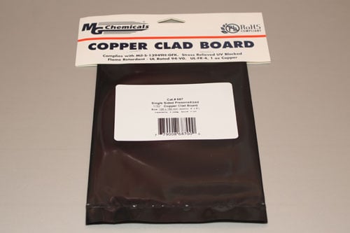
The board used in this project is made by MG Chemicals and is their Model 687 which is a Single Sided Pre-sensitized 1/32″ Copper Clad Board 100mm x 150mm (approximately 4″ x 6″). This model of the board comes pre-sensitized and incorporates a peel-off layer protecting the sensitized copper base.
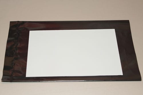
When you remove the pre-sensitized board from the light-protective bag, the board with the sensitized side will have a light plastic protective covering on it.
Remember that the board is light-sensitive. You should use caution when preparing the material to limit exposure to ambient light.
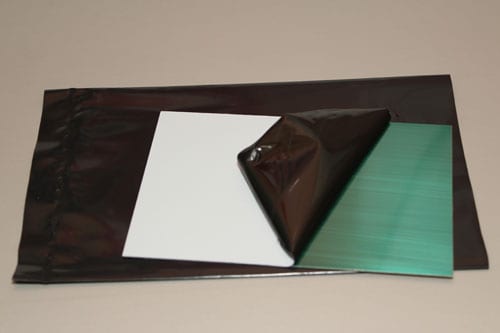
Slowly peel the protective coating from the board.
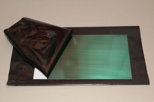
Slowly peel the protective coating from the board.
Once you have the protective covering removed from the sensitized side of the board, you are ready to begin the exposure process.
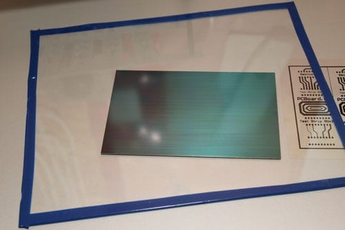
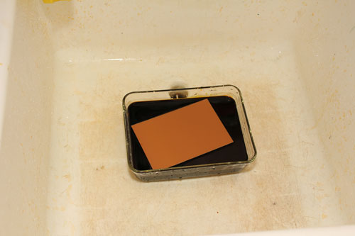
Now would be a good time to ensure your positive film you have created fits the size of PC board you selected. In our case, a perfect fit.
Now would be a good time to ensure your positive film you have created fits the size of PC board you selected. In our case, a perfect fit.
Exposing the left-most area of the board for 15 seconds.
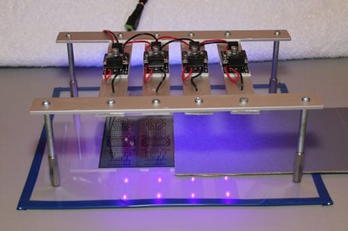
Now slide the card to expose the second area for 15 seconds.
Now slide the card to expose the third area for 15 seconds.
After another 15 seconds, expose the last section of the board. In total, the leftmost area of the board has now been exposed for 60 seconds.
The board has now been exposed. The leftmost area of the board was exposed for 60 seconds, while second from the left for 45 seconds, second to the right area for 40 seconds and finally the rightmost area for 15 seconds.
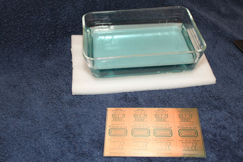
You can now remove the artwork from on top of the board. There is nothing visible on the surface yet. The board must now be developed where the areas exposed to the UV light will be developed and removed. Unexposed areas will turn black.
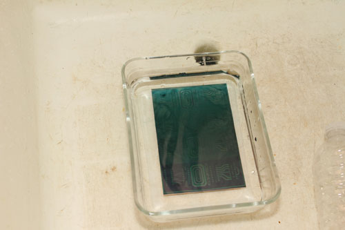
Developing of the board only takes a few minutes. Slide the board into the Positive Developer solution without splashing it around.
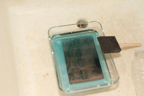
To help the developing process, lightly wipe the top of the board with a foam brush to assist the resist in coming off the board.
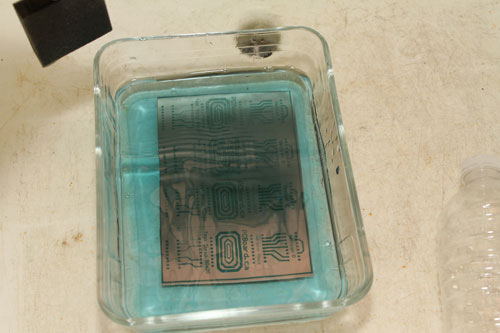
Within a minute, your board should be fully developed. A very quick process and the results can be seen almost immediately.
After fully developing your board, rinse it off well under warm running water for about a minute to remove all chemical residue.
Once the board has been developed, it is time to actually etch the image into the copper. From the exposed board, wherever light was able to hit the board, this will result in the copper being removed.
The etchant being used is Ferric Chloride. The board can either be floated on the surface, with the copper side facing down, or sunk into the etchant.
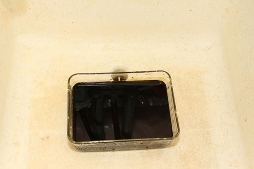
The etching process will take a few minutes to completely remove the photo-sensitized exposed area. Immerse the copper board, copper side down, in the Ferric Chloride solution and agitate until etching action is completed.
The etching process can be sped up by heating the Ferric Chloride solution to a temperature no higher than 55C (135F).
When the etching process is complete, remove the board from the Ferric Chloride etchant bath and rinse with water. The board still has the photographic mask on the copper sections. This is removed with Acetone (common nail polish remover), and finally with a rinse of water.
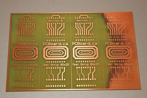
After the photographic mask is removed from the PCB, you are left with a copper PCB pattern of your circuit. We can see the optimal exposure occurs in the second from the right section. This had an exposure of 30 seconds.
Final drilling of the PCB can now be undertaken to finish off the board.
The UV Exposer system has been in operation since April 2012. As of the writing of this article, about 180 boards have been exposed and developed, each for a custom design. Exposer time has been standardized to 20 seconds per board using the UV LEDs and 1 watt LED Driver.
The developing process has undergone one change. The Ferric Chloride has now been replaced by Ammonium Persulphate and a move to Sodium Persulphate is expected soon.
Ferric Chloride has a nasty tendency to stain anything it touches, including clothing and your fingers. Ammonium Persulphate is much easier to handle, shows when the liquid is saturated with copper, but some of the boards have added artwork using an Etch Pen (which is a Venus Sharpe indelible ink marker). There is conflicting information on whether Sodium Persulphate is or is not compatible with the Etch Pen, so testing will need to be done.
A final note. Care must be taken when using an apparatus like this due to the UV light being emitted. Proper care should be undertaken to protect your eyes.